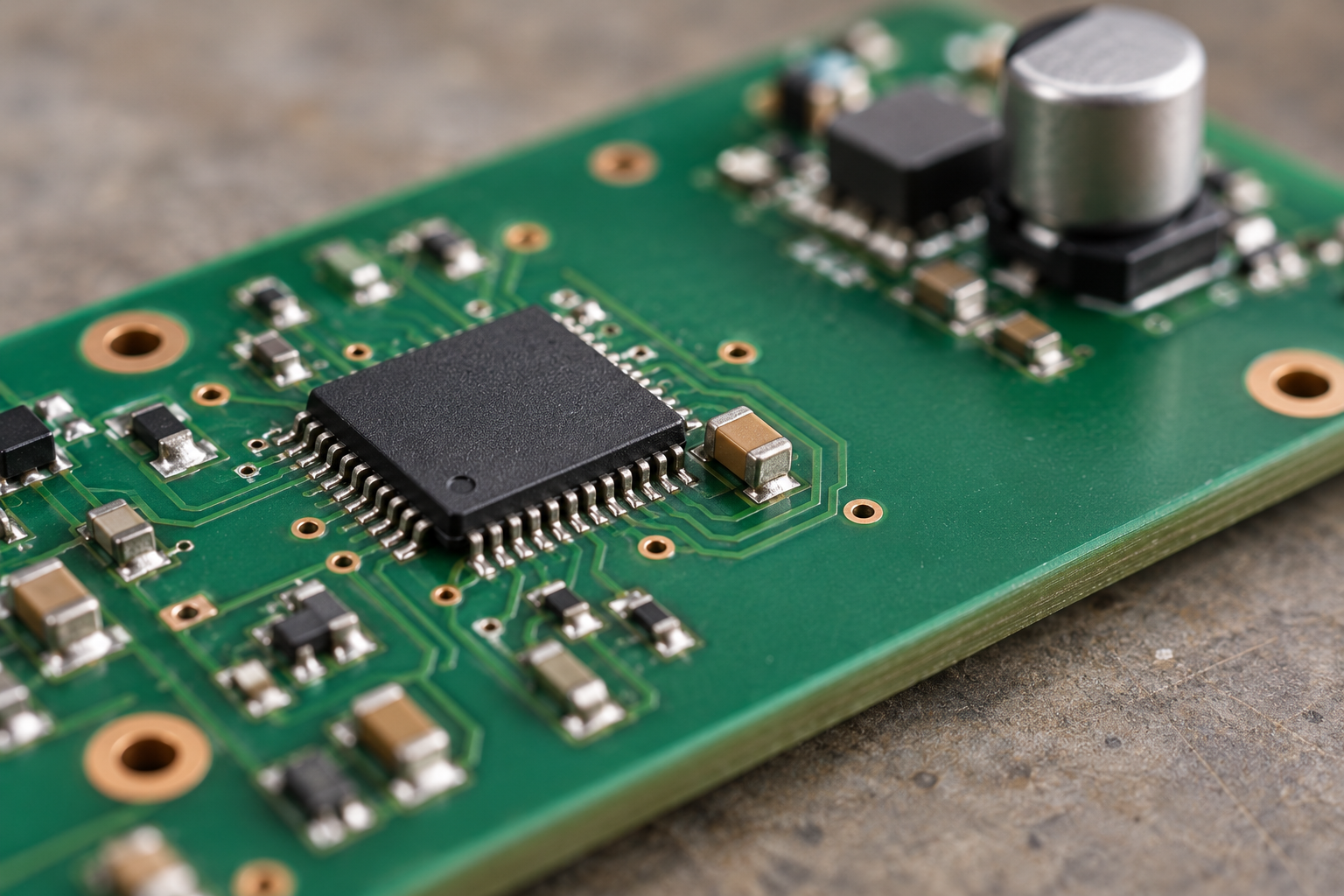
On a circuit diagram, a capacitor drawn beside an integrated circuit looks as though it lives next door. On the board, that symbol can be a long trace, a detour through a via and a distant trip through the ground plane. The chip experiences the route made in copper, not the tidy distance on the page. That is why a decoupling capacitor belongs near its power pin: its job is to provide a short, low-impedance path for current that changes faster than the rest of the supply network can comfortably deliver.
An integrated circuit's current draw is seldom perfectly steady. Digital gates change state; an amplifier drives a changing load; a clocked converter samples and resets. The voltage regulator may be doing its job well at the other end of the board, yet the conductors between it and the chip have resistance and inductance. During a sudden demand, the chip can briefly see its supply voltage sag. When current changes in the other direction, voltage can overshoot or ring. A local capacitor stores a little charge and, more importantly, offers a path with low impedance over the frequencies that matter for that circuit. Texas Instruments' 2020 layout note for a class-D audio amplifier ties pin-level voltage spikes to the resistance and inductance in the complete decoupling path.
The trip out and the trip back
The current loop is the useful thing to picture. Current moves between the capacitor's power side and the chip's supply pin; it must also return between the chip's ground and the capacitor's ground side. Putting the capacitor close to the supply pin while sending its ground connection around the far side of the board gives it a good address and a poor journey. In TI's earlier note on high-speed operational amplifiers, a 14-pin dual-in-line package makes the difficulty visible: power and ground pins can sit at opposite corners. Choosing a location close to one pin leaves a long connection to the other unless the board layout supplies a better return route.
Inductance is why those extra lengths matter during a fast change. The approximate induced voltage across an inductive path is its inductance multiplied by how quickly current changes. As an illustration, a change of 0.1 ampere in one nanosecond across one nanohenry corresponds to 0.1 volt during the change. Those numbers are a thought experiment, not a measured fault or a universal limit. They show why “only a little more copper” can become relevant when the event is brief. TI's device-specific audio layout guide says even nanohenries can affect supply ripple in its fast-switching design, and asks for the smallest local capacitor within a millimetre of the relevant pin. That distance is its target for that amplifier, not a ruler to impose on every hobby circuit.
The return path can be a short trace to the chip's ground pin or a nearby connection to a suitable ground plane, depending on the board. Either way, the loop includes the chip, its package pins, capacitor pads, traces, vias and the return copper. A via is not a portal that erases distance. It adds a small inductance of its own. Altera's board design guidance calls this mounting inductance and adds it to the capacitor's published internal inductance. It recommends placing power and ground vias close to the capacitor pads, using short wide connections and keeping the relevant planes close to the surface where the part is mounted. The nearest-looking part in a photograph may not have the shortest electrical loop.
The capacitor is a real object
The printed value on a capacitor describes its capacitance, but the part also has equivalent series resistance and equivalent series inductance, usually shortened to ESR and ESL. At low enough frequencies, more capacitance generally offers more stored charge and lower capacitive impedance. As frequency rises, the capacitance and ESL meet at the part's self-resonant frequency. Above that point, the inductive behaviour grows. TI's high-speed layout report plots the resulting impedance curves and explains why a physically small, low-inductance capacitor can serve faster changes while a larger one helps at slower ones. A capacitor marked “0.1 µF” is therefore not a complete answer to a power-supply problem. Its package, construction and placement help decide what that value can do on the board.
The division of work is not a rigid rule that every board needs a staircase of values. In Microsemi's 2017 guidance for its clock chips, the local recommendation is one low-ESR 0.1–1 µF capacitor per power pin, close to that pin, plus a 10 µF bulk capacitor for each power domain. It also asks that the local capacitors not share power or ground vias. Those are concrete instructions for those parts. The bulk capacitor and the nearby small ones have related jobs, but the chip's own documentation decides the values and placement priorities. Copying the clock-chip list onto an unrelated sensor would be an act of faith in the wrong document.
More parts can help, but a bag of assorted capacitors is not a substitute for knowing the demand. Analog Devices' 2012 high-speed converter layout note shows that a suitable pair of values can make a power distribution network low in impedance across its target range without populating every intermediate value. It also warns that badly chosen or mounted capacitors can resonate with one another and create an impedance peak. That matters because a circuit can be quiet at some frequencies and unexpectedly vulnerable at another. The aim is a low-impedance supply path across the relevant range, not a satisfying count of beige rectangles beside the chip.
Near is a property of the whole board
The board stack and power source share the work. In TI's 2011 design method for its OMAP-family processors, the regulator, bulk capacitors, local ceramic capacitors and closely spaced power and ground planes cover different parts of the power network's frequency range. The report sets a target impedance for one processor rail and counts capacitor ESL, mounting vias and the spreading path in the board toward a total loop-inductance limit. Its numerical target belongs to that processor and its assumed current and voltage tolerance. The broader principle is that a capacitor soldered against a chip cannot compensate for an ill-chosen path beneath it.
This also explains why “as close as possible” is a design instruction rather than a magic measurement. Before deciding where a capacitor goes, identify the exact power and ground pins and the rail it serves. Read that component's power recommendations. Then trace the short outgoing and return paths on the actual layout, including vias and plane connections. A larger reservoir may sit at the entrance to a power domain, while a small local part takes priority beside a pin with rapid current demands. For a crowded or high-speed board, the power-network impedance may need calculation, simulation or measurement rather than another guess. The documentation for the actual chip and the actual board geometry decide how much is enough.
The little ceramic package is easy to treat as an afterthought because its schematic symbol is so simple. Its location is part of its electrical performance. Move it away, lengthen its return, or bury its connection behind unnecessary inductance, and the component with the correct printed value can become the wrong answer. The board is where “near” acquires a meaning the chip can use.

A thought worth keeping?